Harvesting Water With High Voltage

Atmospheric water harvesting is a way to obtain fresh water in arid regions, as there is always some moisture in the air, especially in the form of morning fog. The trick lies in capturing this moisture as efficiently as possible, with a range of methods available that start at ancient low-tech methods involving passive fog droplet capture all the way to variants of what are effectively large dehumidifiers.

A less common way involves high-voltage and found itself the subject of a recent Plasma Channel video on YouTube. The inspiration for the build was a 2018 paper by [Maher Damak] et al. (PDF) titled Electrostatically driven fog collection using space charge injection.

One of the two stakes that make up the electrostatic precipitator system for atmospheric water harvesting. (Credit: Plasma Channel, YouTube)

Rather than passively waiting for dew to collect on the collector, as with many of the methods detailed in this review article by [Xiaoyi Liu] et al., this electrostatic approach pretty much does what it says on the tin. It follows the principle of electrostatic precipitators with a high-voltage emitter electrode to ionize the air and grounded collector wires. In the video a small-scale version (see top image) was first constructed, demonstrating the effectiveness. Whereas the passive grid collected virtually none of the fog from an ultrasonic fog maker, with 35 kV applied the difference was night and day. No water was collected with the first test, but with power applied a significant 40 mL was collected in 5 minutes on the small mesh.

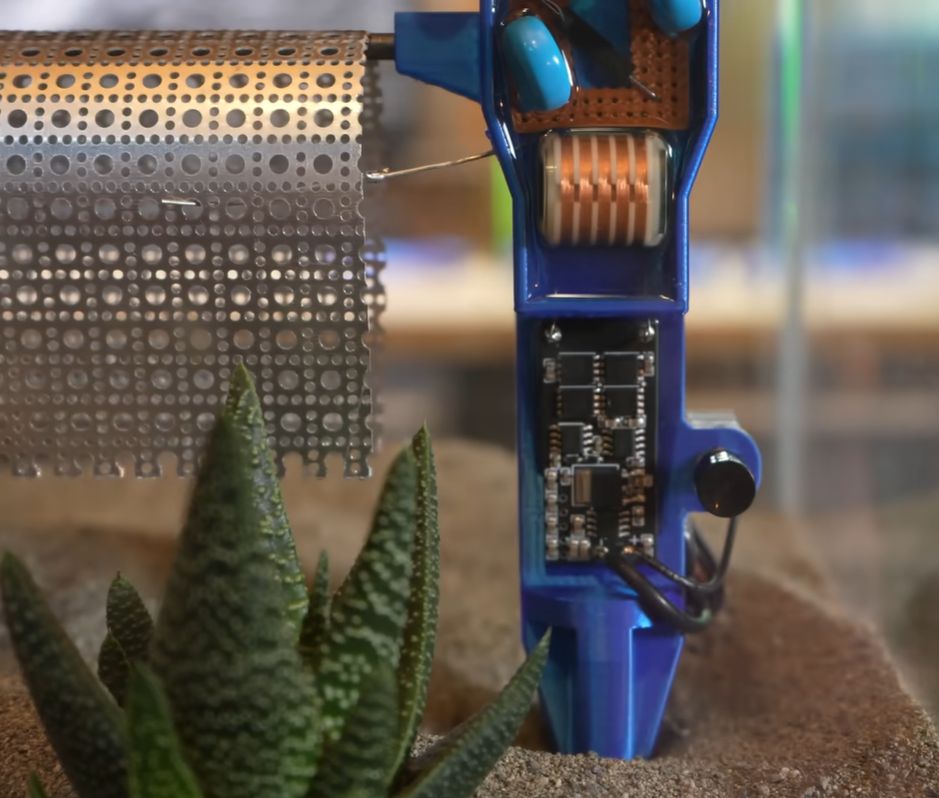
With this scale test complete, a larger version could be designed and tested. This simplifies the emitter to a single wire connected between two stakes, one of which contains the 20 kV HV generator and battery. The mesh is placed right below it and grounded (see image). With an extreme fog test inside a terrarium, it showed a very strong effect, resulting in a harvest of 14 mL/Wh for this prototype. With a larger scale version in a real-life environment (i.e. desert) planned, it’ll be interesting to see whether this method holds up in a more realistic scenario.

Continue reading “Harvesting Water With High Voltage”

How Rutherford Proved That Atoms Are Mostly Empty Space

By the beginning of the 20th century scientists were only just beginning to probe the mysteries of the atomic world, with the exact nature of these atoms subject to a lot of speculation and theory. Recently [The Action Lab] on YouTube replicated one of the most famous experiments performed at the time, commonly known as Rutherford’s gold-foil experiment.

A part of Rutherford’s scattering experiments, this particular experiment involved shooting alpha particles at a piece of gold foil with the source, foil, and detector placed in a vacuum vessel. Rutherford’s theoretical model of the atom that he developed over the course of these experiments differed from the contemporary Thomson model in that Rutherford’s model postulated that atoms consisted of a single large charged nucleus at the core of the atom, with the electrons spread around it.

As can be seen in the video, the relatively large alpha particles from the Americium-241 source, available from many smoke detectors, will most of the time zip right through the foil, while suffering a pretty major deflection in other times when a nucleus is hit. This is consistent with Rutherford’s model of a small nucleus surrounded by what is effectively mostly just empty space.

While Rutherford used a screen that would light up when hit with alpha particles, this experiment with a Geiger counter is an easy way to replicate the experiment, assuming that you have access to a large enough vacuum chamber.

Continue reading “How Rutherford Proved That Atoms Are Mostly Empty Space”

Schematic of a circuit

Hacking Flux Paths: The Surprising Magnetic Bypass

If you think shorting a transformer’s winding means big sparks and fried wires: think again. In this educational video, titled The Magnetic Bypass, [Sam Ben-Yaakov] flips this assumption. By cleverly tweaking a reluctance-based magnetic circuit, this hack channels flux in a way that breaks the usual rules. Using a simple free leg and a switched winding, the setup ensures that shorting the output doesn’t spike the current. For anyone who is obsessed with magnetic circuits or who just loves unexpected engineering quirks, this one is worth a closer look.

So, what’s going on under the hood? The trick lies in flux redistribution. In a typical transformer, shorting an auxiliary winding invites a surge of current. Here, most of the flux detours through a lower-reluctance path: the magnetic bypass. This reduces flux in the auxiliary leg, leaving voltage and current surprisingly low. [Sam]’s simulations in LTspice back it up: 10 V in yields a modest 6 mV out when shorted. It’s like telling flux where to go, but without complex electronics. It is a potential stepping stone for safer high-voltage applications, thanks to its inherent current-limiting nature.

The original video walks through the theory, circuit equivalences, and LTspice tests. Enjoy!

Continue reading “Hacking Flux Paths: The Surprising Magnetic Bypass”

Microsoft (Again) Claims Topological Quantum Computing With Majorana Zero Mode Anyons

As the fundamental flaw of today’s quantum computers, improving qubit stability remains the focus of much research in this field. One such stability attempt involves so-called topological quantum computing with the use of anyons, which are two-dimensional quasiparticles. Such an approach has been claimed by Microsoft in a recent paper in Nature. This comes a few years after an earlier claim by Microsoft for much the same feat, which was found to be based on faulty science and hence retracted.

The claimed creation of anyons here involves Majorana fermions, which differ from the much more typical Dirac fermions. These Majorana fermions are bound with other such fermions as a Majorana zero mode (MZM), forming anyons that are intertwined (braided) to form what are in effect logic gates. In the Nature paper the Microsoft researchers demonstrate a superconducting indium-arsenide (InAs) nanowire-based device featuring a read-out circuit  (quantum dot interferometer) with the capacitance of one of the quantum dots said to vary in a way that suggests that the nanowire device-under-test demonstrates the presence of MZMs at either end of the wire.

Microsoft has a dedicated website to their quantum computing efforts, though it remains essential to stress that this is not a confirmation until their research is replicated by independent researchers. If confirmed, MZMs could provide a way to create more reliable quantum computing circuitry that does not have to lean so heavily on error correction to get any usable output. Other, competing efforts here include such things as hybrid mechanical qubits and antimony-based qubits that should be more stable owing to their eight spin configurations.

Pulsed Deposition Points A Different Path To DIY Semiconductors

While not impossible, replicating the machines and processes of a modern semiconductor fab is a pretty steep climb for the home gamer. Sure, we’ve seen it done, but nanoscale photolithography is a demanding process that discourages the DIYer at every turn. So if you want to make semiconductors at home, it might be best to change the rules a little and give something like this pulsed laser deposition prototyping apparatus a try.

Rather than building up a semiconductor by depositing layers of material onto a silicon substrate and selectively etching features into them with photolithography, [Sebastián Elgueta]’s chips will be made by adding materials in their final shape, with no etching required. The heart of the process is a multi-material pulsed laser deposition chamber, which uses an Nd:YAG laser to ablate one of six materials held on a rotating turret, creating a plasma that can be deposited onto a silicon substrate. Layers can either be a single material or, with the turret rapidly switched between different targets, a mix of multiple materials. The chamber is also equipped with valves for admitting different gases, such as oxygen when insulating layers of metal oxides need to be deposited. To create features, a pattern etched into a continuous web of aluminum foil by a second laser is used as a mask. When a new mask is needed, a fresh area of the foil is rolled into position over the substrate; this keeps the patterns in perfect alignment.

We’ve noticed regular updates on this project, so it’s under active development. [Sebastián]’s most recent improvements to the setup have involved adding electronics inside the chamber, including a resistive heater to warm the substrate before deposition and a quartz crystal microbalance to measure the amount of material being deposited. We’re eager to see what else he comes up with, especially when those first chips roll off the line. Until then, we’ll just have to look back at some of [Sam Zeloof]’s DIY semiconductors.

MIT Demonstrates Fully 3D Printed, Active Electronic Components

One can 3D print with conductive filament, and therefore plausibly create passive components like resistors. But what about active components, which typically require semiconductors? Researchers at MIT demonstrate working concepts for a resettable fuse and logic gates, completely 3D printed and semiconductor-free.

Now just to be absolutely clear — these are still just proofs of concept. To say they are big and perform poorly compared to their semiconductor equivalents would be an understatement. But they do work, and they are 100% 3D printed active electronic components, using commercially-available filament.

How does one make a working resettable fuse and transistor out of such stuff? By harnessing thermal expansion, essentially.

Continue reading “MIT Demonstrates Fully 3D Printed, Active Electronic Components”

Measuring Local Variances In Earth’s Magnetic Field

Although the Earth’s magnetic field is reliable enough for navigation and is also essential for blocking harmful solar emissions and for improving radio communications, it’s not a uniform strength everywhere on the planet. Much like how inconsistencies in the density of the materials of the planet can impact the local gravitational force ever so slightly, so to can slight changes impact the strength of the magnetic field from place to place. And it doesn’t take too much to measure this impact on your own, as [efeyenice983] demonstrates here.

To measure this local field strength, the first item needed is a working compass. With the compass aligned to north, a magnet is placed with its poles aligned at a right angle to the compass. The deflection angle of the needle is noted for varying distances of the magnet, and with some quick math the local field strength of the Earth’s magnetic field can be calculated based on the strength of the magnet and the amount of change of the compass needle when under its influence.

Using this method, [efeyenice983] found that the Earth’s magnetic field strength at their location was about 0.49 Gauss, which is well within 0.25 to 0.65 Gauss that is typically found on the planet’s surface. Not only does the magnetic field strength vary with location, it’s been generally decreasing in strength on average over the past century or so as well, and the poles themselves aren’t stationary either. Check out this article which shows just how much the poles have shifted over the last few decades.